|
|
PDF IS61QDB22M18 Data sheet ( Hoja de datos )
| Número de pieza | IS61QDB22M18 | |
| Descripción | QUAD (Burst of 2) Synchronous SRAMs | |
| Fabricantes | ISSI | |
| Logotipo |  |
|
Hay una vista previa y un enlace de descarga de IS61QDB22M18 (archivo pdf) en la parte inferior de esta página. Total 27 Páginas | ||
|
No Preview Available !
36 Mb (1M x 36. & 2M x 18)
QUAD (Burst of 2) Synchronous SRAMs
I
Features
• 1M x 36 or 2M x 18.
• On-chip delay-locked loop (DLL) for wide data
valid window.
• Separate read and write ports with concurrent
read and write operations.
• Synchronous pipeline read with early write oper-
ation.
• Double data rate (DDR) interface for read and
write input ports.
• Fixed 2-bit burst for read and write operations.
• Clock stop support.
• Two input clocks (K and K) for address and con-
trol registering at rising edges only.
• Two input clocks (C and C) for data output con-
trol.
JANUARY 2010
• Two echo clocks (CQ and CQ) that are delivered
simultaneously with data.
• +1.8V core power supply and 1.5, 1.8V VDDQ,
used with 0.75, 0.9V VREF.
• HSTL input and output levels.
• Registered addresses, write and read controls,
byte writes, data in, and data outputs.
• Full data coherency.
• Boundary scan using limited set of JTAG 1149.1
functions.
• Byte write capability.
• Fine ball grid array (FBGA) package
- 15mm x 17mm body size
- 1mm pitch
- 165-ball (11 x 15) array
• Programmable impedance output drivers via 5x
user-supplied precision resistor.
Description
The 36Mb IS61QDB21Mx36 and IS61QDB22Mx18
are synchronous, high-performance CMOS static
random access memory (SRAM) devices. These
These SRAMs have separate I/Os, eliminating the
need for high-speed bus turnaround. The rising
edge of K clock initiates the read/write operation,
and all internal operations are self-timed. Refer to
the Timing Reference Diagram for Truth Table
on page 8 for a description of the basic opera-
tions of these SRAMs.
The input address bus operates at double data rate.
The following are registered internally on the rising
edge of the K clock:
• Read address
• Read enable
• Write enable
• Byte writes
• Data-in for early writes
The following are registered on the rising edge of
the K clock:
• Write address
• Byte writes
• Data-in for second burst addresses
Byte writes can change with the corresponding data-
in to enable or disable writes on a per-byte basis. An
internal write buffer enables the data-ins to be regis-
tered half a cycle earlier than the write address. The
first data-in burst is clocked at the same time as the
write command signal, and the second burst is timed
to the following rising edge of the K clock.
During the burst read operation, the data-outs from
the first burst are updated from output registers off
the second rising edge of the C clock (1.5 cycles
later). The data-outs from the second burst are
updated with the third rising edge of the C clock. The
K and K clocks are used to time the data-outs when-
ever the C and C clocks are tied high.
The device is operated with a single +1.8V power
supply and is compatible with HSTL I/O interfaces.
Integrated Silicon Solution, Inc. — 1-800-379-4774
Rev. H
1/6/2010
1
1 page 
36 Mb (1M x 36 & 2M x 18)
QUAD (Burst of 2) Synchronous SRAMs
ISSI®
During a write, the byte writes independently control which byte of any of the two burst addresses is written
(see X18/X36 Write Truth Tables on page 9 and Timing Reference Diagram for Truth Table on page 8).
Whenever a write is disabled (W is high at the rising edge of K), data is not written into the memory.
RQ Programmable Impedance
An external resistor, RQ, must be connected between the ZQ pin on the SRAM and VSS to enable the SRAM
to adjust its output driver impedance. The value of RQ must be 5x the value of the intended line impedance
driven by the SRAM. For example, an RQ of 250Ω results in a driver impedance of 50Ω. The allowable range
of RQ to guarantee impedance matching is between 175Ω and 350Ω, with the tolerance described in
Programmable Impedance Output Driver DC Electrical Characteristics on page 13. The RQ resistor should
be placed less than two inches away from the ZQ ball on the SRAM module. The capacitance of the loaded
ZQ trace must be less than 3 pF.
The ZQ pin can also be directly connected to VDDQ to obtain a minimum impedance setting. ZQ must never
be connected to VSS.
Programmable Impedance and Power-Up Requirements
Periodic readjustment of the output driver impedance is necessary as the impedance is greatly affected by
drifts in supply voltage and temperature. At power-up, the driver impedance is in the middle of allowable
impedances values. The final impedance value is achieved within 1024 clock cycles.
Clock Consideration
This device uses an internal DLL for maximum output data valid window. It can be placed in a stopped-clock
mode to minimize power and requires only 1024 cycles to restart.
No clocks can be issued until VDD reaches its allowable operating range.
Single Clock Mode
This device can be also operated in single-clock mode. In this case, C and C are both connected high at
power-up and must never change. Under this condition, K and K will control the output timings.
Either clock pair must have both polarities switching and must never connect to VREF, as they are not differ-
ential clocks
Depth Expansion
Separate input and output ports enable easy depth expansion, as each port can be selected and deselected
independently. Read and write operations can occur simultaneously without affecting each other. Also, all
pending read and write transactions are always completed prior to deselecting the corresponding port.
In the following application example, the second pair of C and C clocks is delayed such that the return data
meets the data setup and hold times at the bus master.
Integrated Silicon Solution, Inc. — 1-800-379-4774
Rev. H
1/6/2010
5
5 Page 
36 Mb (1M x 36 & 2M x 18)
QUAD (Burst of 2) Synchronous SRAMs
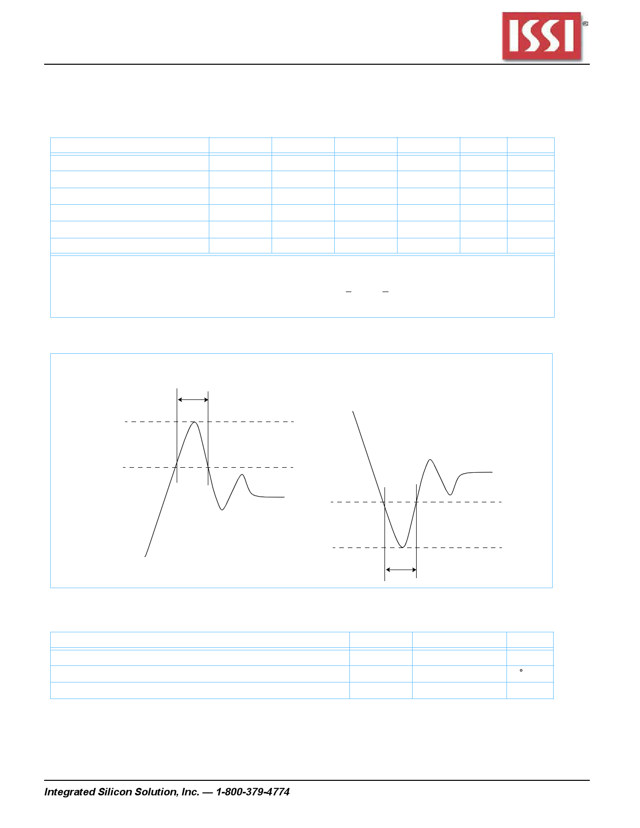
Recommended DC Operating Conditions (Over the operating temperature)
Parameter
Symbol
Minimum
Typical
Maximum
Supply voltage
Output driver supply voltage
Input high voltage
Input low voltage
Input reference voltage
Clocks signal voltage
VDD
VDDQ
VIH
VIL
VREF
VIN - CLK
1.8 - 5%
1.4
VREF +0.1
-0.3
0.68
-0.3
1.8 + 5%
1.9
VDDQ + 0.3
VREF - 0.1
0.95
VDDQ + 0.3
1. All voltages are referenced to VSS. All VDD, VDDQ, and VSS pins must be connected.
2. VIH(Max) AC = See 0vershoot and Undershoot Timings.
3. VIL(Min) AC = See 0vershoot and Undershoot Timings.
4. VIN-CLK specifies the maximum allowable DC excursions of each clock (K, K, C, and C).
5. Peak-to-peak AC component superimposed on VREF may not exceed 5% of VREF.
0vershoot and Undershoot Timings
Units
V
V
V
V
V
V
Notes
1
1
1, 2
1, 3
1, 5
1, 4
20% Min Cycle Time
VDDQ+0.6V
VIL(Min) AC
Undershoot Timing
VDDQ
VIH(Max) AC
Overshoot Timing
GND
GND-0.6V
20% Min Cycle Time
PBGA Thermal Characteristics
Item
Thermal resistance junction to ambient (airflow = 1m/s)
Thermal resistance junction to case
Thermal resistance junction to pins
Symbol
RΘJA
RΘJC
RΘJB
Rating
20.4
4.0
3.23
Units
° C/W
C/W
°C/W
Integrated Silicon Solution, Inc. — 1-800-379-4774
Rev. H
1/6/2010
11
11 Page | ||
| Páginas | Total 27 Páginas | |
| PDF Descargar | [ Datasheet IS61QDB22M18.PDF ] | |
Hoja de datos destacado
| Número de pieza | Descripción | Fabricantes |
| IS61QDB22M18 | QUAD (Burst of 2) Synchronous SRAMs | ISSI |
| IS61QDB22M18A | 36Mb QUAD (Burst 2) Synchronous SRAM | ISSI |
| Número de pieza | Descripción | Fabricantes |
| SLA6805M | High Voltage 3 phase Motor Driver IC. |
Sanken |
| SDC1742 | 12- and 14-Bit Hybrid Synchro / Resolver-to-Digital Converters. |
Analog Devices |
|
DataSheet.es es una pagina web que funciona como un repositorio de manuales o hoja de datos de muchos de los productos más populares, |
| DataSheet.es | 2020 | Privacy Policy | Contacto | Buscar |
