|
|
|
PDF IS65WV12816BLL Data sheet ( Hoja de datos )
| Número de pieza | IS65WV12816BLL | |
| Descripción | ULTRA LOW POWER CMOS STATIC RAM | |
| Fabricantes | ISSI | |
| Logotipo | ||
Hay una vista previa y un enlace de descarga de IS65WV12816BLL (archivo pdf) en la parte inferior de esta página. Total 19 Páginas | ||
|
No Preview Available !
IS65WV12816ALL
IS65WV12816BLL
ISSI®
128K x 16 LOW VOLTAGE,
ULTRA LOW POWER CMOS STATIC RAM
PRELIMINARY INFORMATION
JUNE 2006
FEATURES
• High-speed access time: 55ns, 70ns
• CMOS low power operation:
36 mW (typical) operating
9 µW (typical) CMOS standby
• TTL compatible interface levels
• Single power supply:
1.65V to 2.2V VDD (65WV12816ALL)
2.5V to 3.6V VDD (65WV12816BLL)
• Fully static operation: no clock or refresh
required
• Three state outputs
• Data control for upper and lower bytes
• 2CS Option Available
• Temperature Offerings:
Option A: 0 to 70oC
Option A1: –40 to +85oC
Option A2: –40 to +105oC
Option A3: –40 to +125oC
• Lead-free available
DESCRIPTION
The ISSI IS65WV12816ALL/ IS65WV12816BLL are high-
speed, 2M bit static RAMs organized as 128K words by 16
bits. It is fabricated using ISSI's high-performance CMOS
technology. This highly reliable process coupled with
innovative circuit design techniques, yields high-
performance and low power consumption devices.
When CS1 is HIGH (deselected) or when CS2 is LOW
(deselected) or when CS1 is LOW, CS2 is HIGH and both
LB and UB are HIGH, the device assumes a standby mode
at which the power dissipation can be reduced down with
CMOS input levels.
Easy memory expansion is provided by using Chip Enable
and Output Enable inputs. The active LOW Write Enable
(WE) controls both writing and reading of the memory. A
data byte allows Upper Byte (UB) and Lower Byte (LB)
access.
The IS65WV12816ALL and IS65WV12816BLL are packged
in the JEDEC standard 48-pin mini BGA (6mm x 8mm) and
44-Pin TSOP (TYPE II).
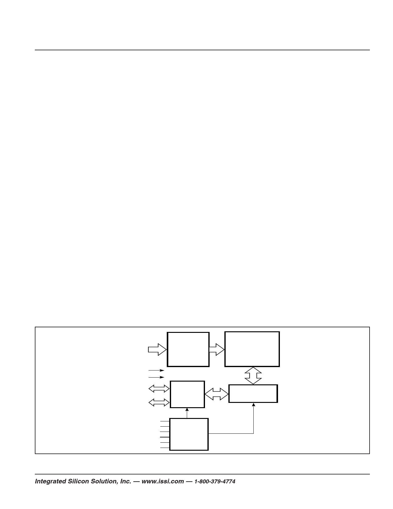
FUNCTIONAL BLOCK DIAGRAM
A0-A16
DECODER
128K x 16
MEMORY ARRAY
VDD
GND
I/O0-I/O7
Lower Byte
I/O8-I/O15
Upper Byte
I/O
DATA
CIRCUIT
COLUMN I/O
CS2
CS1
OE
WE
UB
LB
CONTROL
CIRCUIT
Copyright © 2006 Integrated Silicon Solution, Inc. All rights reserved. ISSI reserves the right to make changes to this specification and its products at any time without notice. ISSI assumes no liability
arising out of the application or use of any information, products or services described herein. Customers are advised to obtain the latest version of this device specification before relying on any
published information and before placing orders for products.
Integrated Silicon Solution, Inc. — www.issi.com — 1-800-379-4774
Rev. 00E
06/08/06
1
1 page 
IS65WV12816ALL, IS65WV12816BLL
ISSI®
IS65WV12816ALL, POWER SUPPLY CHARACTERISTICS(1) (Over Operating Range)
Symbol Parameter
Test Conditions
Options
ICC VddDynamicOperating VDD=Max.,
SupplyCurrent
IOUT = 0 mA, f = fMAX
ICC1 OperatingSupply
VDD = Max.,
Current
IOUT = 0 mA, f = 0
ISB1 TTLStandbyCurrent
VDD = Max.,
(TTL Inputs)
VIN = VIH or VIL
CS1 = VIH , CS2 = VIL,
f = 1 MHZ
OR
A,A1
A2,A3
A,A1
A2,A3
A,A1
A2,A3
ULB Control
VDD= Max., VIN = VIH or VIL
CS1 = VIL, f = 0, UB = VIH, LB = VIH
ISB2 CMOSStandby
VDD = Max.,
Current(CMOSInputs) CS1≥ VDD–0.2V,
CS2 ≤ 0.2V,
VIN ≥ VDD – 0.2V,or
VIN ≤ 0.2V, f = 0 OR
A,A1
A2
A3
ULB Control
VDD = Max., CS1 = VIL, CS2=VIH
VIN ≤ 0.2V, f = 0; UB / LB = VDD – 0.2V
Max.
-70 ns
15
20
7
7
0.6
0.6
Unit
mA
mA
mA
15 µA
20
50
IS65WV12816BLL, POWER SUPPLY CHARACTERISTICS(1) (Over Operating Range)
Symbol Parameter
Test Conditions
ICC VddDynamicOperating VDD=Max.,
SupplyCurrent
IOUT = 0 mA, f = fMAX
ICC1 OperatingSupply
VDD = Max.,
Current
IOUT = 0 mA, f = 0
ISB1 TTLStandbyCurrent
VDD = Max.,
(TTL Inputs)
VIN = VIH or VIL
CS1 = VIH , CS2 = VIL,
f = 1 MHZ
OR
Options
A,A1
A2,A3
A,A1
A2,A3
A,A1
A2,A3
Max.
-55 ns
25
30
7
7
0.6
0.6
Max.
-70 ns
20
25
7
7
0.6
0.6
Unit
mA
mA
mA
ULB Control
VDD= Max., VIN = VIH or VIL
CS1 = VIL, f = 0, UB = VIH, LB = VIH
ISB2 CMOSStandby
VDD = Max.,
Current(CMOSInputs) CS1≥ VDD–0.2V,
CS2 ≤ 0.2V,
VIN ≥ VDD – 0.2V,or
VIN ≤ 0.2V, f = 0
OR
A,A1
A2
A3
15 15 µA
25 25
65 65
ULB Control
VDD = Max., CS1 = VIL, CS2=VIH
VIN ≤ 0.2V, f = 0; UB / LB = VDD – 0.2V
Note:
1. At f = fMAX, address and data inputs are cycling at the maximum frequency, f = 0 means no input lines change.
Integrated Silicon Solution, Inc. — www.issi.com — 1-800-379-4774
Rev. 00E
06/08/06
5
5 Page 
IS65WV12816ALL, IS65WV12816BLL
AC WAVEFORMS
WRITE CYCLE NO. 2 (WE Controlled: OE is HIGH During Write Cycle)
ADDRESS
tWC
OE
CS1
CS2
WE
tSCS1
tSCS2
tAW
t PWE
tHA
LB, UB
DOUT
DIN
tSA tHZWE
DATA UNDEFINED
HIGH-Z
tLZWE
tSD tHD
DATA-IN VALID
ISSI®
Integrated Silicon Solution, Inc. — www.issi.com — 1-800-379-4774
Rev. 00E
06/08/06
11
11 Page | ||
| Páginas | Total 19 Páginas | |
| PDF Descargar | [ Datasheet IS65WV12816BLL.PDF ] | |
Hoja de datos destacado
| Número de pieza | Descripción | Fabricantes |
| IS65WV12816BLL | ULTRA LOW POWER CMOS STATIC RAM | ISSI |
| Número de pieza | Descripción | Fabricantes |
| SLA6805M | High Voltage 3 phase Motor Driver IC. |
Sanken |
| SDC1742 | 12- and 14-Bit Hybrid Synchro / Resolver-to-Digital Converters. |
Analog Devices |
|
DataSheet.es es una pagina web que funciona como un repositorio de manuales o hoja de datos de muchos de los productos más populares, |
| DataSheet.es | 2020 | Privacy Policy | Contacto | Buscar |