|
|
|
PDF RT8562B Data sheet ( Hoja de datos )
| Número de pieza | RT8562B | |
| Descripción | High Voltage 8-CH LED Driver | |
| Fabricantes | Richtek | |
| Logotipo | ||
Hay una vista previa y un enlace de descarga de RT8562B (archivo pdf) en la parte inferior de esta página. Total 13 Páginas | ||
|
No Preview Available !
RT8562B
High Voltage 8-CH LED Driver
General Description
The RT8562B is a 40V 8-CH LED driver capable of
delivering 30mA to each channel with 10 LEDs (3.6V per
diode), total of 80 LEDs with one driver. The RT8562B is
a current mode boost converter opearated at 1MHz, wide
VIN range covers from 4.5V to 24V and the on-chip current
switch is rated at 2.5A.
The PWM output voltage loop regulates the LED pins to
0.6V with an auto-adjustment circuit allowing voltage
mismatches between LED strings. The RT8562B automati-
cally detects and disconnects any unconnected and/or
broken strings during operation from PWM loop to prevent
VOUT from over voltage.
The 1.5% matched LED currents on all channels are simply
programmed with a resistor or a current sink. A very high
contrast ratio true digital PWM dimming can be achieved
by driving PWM pin with a PWM signal.
Other protecting features include programmable output
over voltage protection, LED curren limit, PWM switch
current limit and thermal shutdown.
The RT8562B is packaged with a tiny footprint package of
WQFN-24L 4x4 packages.
Ordering Information
RT8562B
Package Type
QW : WQFN-24L 4x4 (W-Type)
Lead Plating System
G : Green (Halogen Free and Pb Free)
Note :
Richtek products are :
` RoHS compliant and compatible with the current require-
ments of IPC/JEDEC J-STD-020.
` Suitable for use in SnPb or Pb-free soldering processes.
Marking Information
For marking information, contact our sales representative
directly or through a Richtek distributor located in your
area.
Features
z High Voltage : VIN up to 24V, VOUT up to 40V, Driving
up to 80 x 3.6V LEDs (10 each channel)
z Channel Current Programmabe 10mA to 30mA and
Matched to 1.5%
z Current Mode PWM 1MHz Boost Converter
z Easy and High Accuracy Digital Dimming by PWM
Signal
z Programmable Soft-Start
z Automatic Detecting Unconnected and/or Broken
Channel
z Programmable Over Voltage Protection
z Disconnects LED in Shutdown
z VIN Under Voltage Lockout
z Over Temperature Protection
z Current Limiting Protection
z Small 24-Lead WQFN Package
z RoHS Compliant and Halogen Free
Applications
z UMPC and Notebook Computer Backlight
z GPS, Portable DVD Backlight
z Desk Lights and Room Lighting
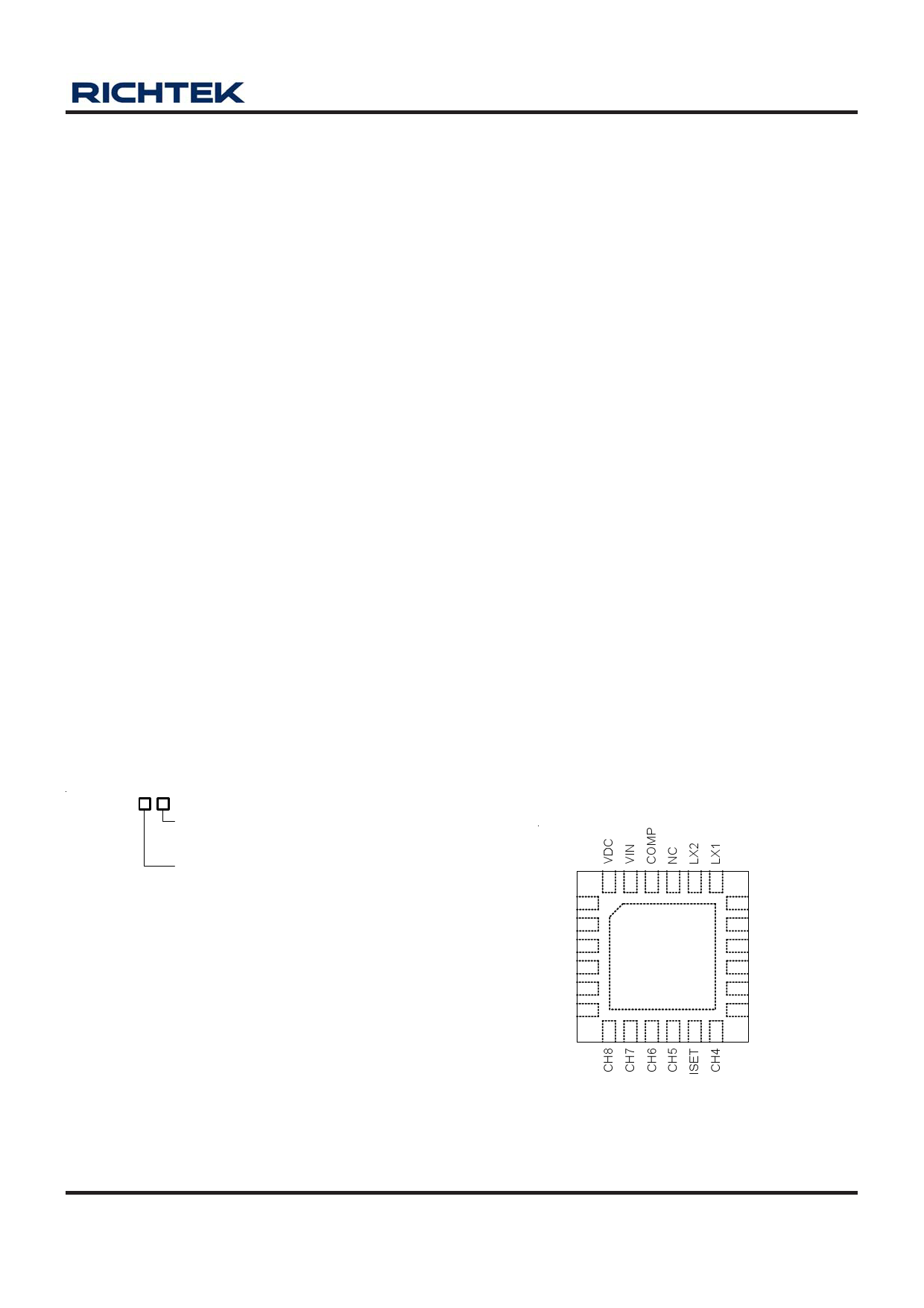
Pin Configurations
(TOP VIEW)
24 23 22 21 20 19
EN 1
18 PGND2
NC 2
17 PGND1
SS 3
NC 4
GND
16 OVP
15 CH1
GND 5
PWM 6
14 CH2
25 13 CH3
7 8 9 10 11 12
WQFN-24L 4x4
DS8562B-06 June 2011
www.richtek.com
1
1 page 
RT8562B
Parameter
PWM Boost Converter
Switching Frequency
Minimum On Time
Regulated VCHx
Amplifier (gm) Output Current
COMP Threshold
LX1, LX2 RDS(ON)
LX1, LX2 Current Limit
SW Maximum Duty
OVP & Soft Start
OVP Threshold
OVP Input Current
Soft Start Current
Thermal Shutdown Temperature
Thermal Shutdown Hysteresis
Symbol
Test Conditions
Highest Voltage LED String
2.4V > COMP > 0.2V
PWM Switch Off
ILIM
VOVP
IOVP
IS S
TSD
VOVP ≤ 3V
VSS ≤ 2.5V
Min Typ Max Unit
0.8 1 1.2 MHz
-- 100 --
ns
0.5 0.6 0.7
V
-- ±15 --
μA
0.1 0.2
--
V
-- 0.3 0.5 Ω
2.5 -- -- A
-- 88 -- %
1.1 1.2 1.3
-- -- 50
358
-- 150 --
-- 20 --
V
nA
μA
°C
°C
Note 1. Stresses listed as the above “Absolute Maximum Ratings” may cause permanent damage to the device. These are for
stress ratings. Functional operation of the device at these or any other conditions beyond those indicated in the
operational sections of the specifications is not implied. Exposure to absolute maximum rating conditions for extended
periods may remain possibility to affect device reliability.
Note 2. θJA is measured in the natural convection at TA = 25°C on a high-effective four layers thermal conductivity test board of
JEDEC 51-7 thermal measurement standard. The case point of θJC is on the expose pad for the WQFN package.
Note 3. Devices are ESD sensitive. Handling precaution is recommended.
Note 4. The device is not guaranteed to function outside its operating conditions.
DS8562B-06 June 2011
www.richtek.com
5
5 Page 
RT8562B
Capacitor Selection
The input capacitor reduces current spikes from the input
supply and minimizes noise injection to the converter. For
most applications, a 10μF ceramic capacitor is sufficient.
A value higher or lower may be used depending on the
noise level from the input supply and the input current to
the converter.
It is recommended to choose a ceramic capacitor bases
on the output voltage ripple requirements. The minimum
value of the output capacitor COUT is approximately given
by the following equation :
COUT
=
(VOUT − VIN )×IOUT
η × VRIPPLE × VOUT × f
Thermal Considerations
For continuous operation, do not exceed absolute
maximum junction temperature. The maximum power
dissipation depends on the thermal resistance of the IC
package, PCB layout, rate of surrounding airflow, and
difference between junction and ambient temperature. The
maximum power dissipaton can be calculated by the
following formula :
PD(MAX)
=
TJ(MAX) − TA
θJA
Where TJ(MAX) is the maximum junction temperature, TA is
the ambient temperature, and θJA is the junction to ambient
thermal resistance.
For recommended operating condition specifications of
RT8562B, the maximum junction temperature is 125°C
and TA is the ambient temperature. The junction to ambient
thermal resistance, θJA is layout dependent. For WQFN-
24L 4x4 packages, the thermal resistance, θJA is 52°C/W
on a standard JEDEC 51-7 four-layer thermal test board.
The maximum power dissipaton at TA = 25°C can be
calculated by the following formula :
P
D(MAX)
=
125°C − 25°C
52°C/W
= 1.923W
for WQFN-24 4x4 package
The maximum power dissipation depends on the operating
ambient temperature for fixed TJ(MAX) and thermal
resistance,θJA. For RT8562B package, the derating curbe
in Figure 4 allows the designer to see the effect of rising
ambient temperature on the maximum power dissipation.
Four-Layer PCB
2.0
1.6
1.2
0.8
0.4
0.0
0
25 50 75 100
Ambient Temperature (°C)
125
Figure 4. Derating Curve for RT8562B Package
Layout Guideline
PCB layout is very important to design power switching
converter circuits. The following layout guide lines should
be strictly followed for best performance of the RT8562B.
` The power components L, D1, C1, COUT1 and COUT2 must
be placed as close as possible to reduce the ac current
loop. The PCB trace between power components must
be short and wide as possible due to large current flow
through these trace during operation.
` Place L and D1 connected to LX pin as close as possible.
The trace should be short and wide as possible.
` It is recommend to place C6 close to VIN pin.
` Pin22 is the compensation point to adjust system
stability. Place the compensation components to pin22
as close as possible.
DS8562B-06 June 2011
www.richtek.com
11
11 Page | ||
| Páginas | Total 13 Páginas | |
| PDF Descargar | [ Datasheet RT8562B.PDF ] | |
Hoja de datos destacado
| Número de pieza | Descripción | Fabricantes |
| RT8562 | High Voltage 8 Channel LED Driver | Richtek |
| RT8562B | High Voltage 8-CH LED Driver | Richtek |
| Número de pieza | Descripción | Fabricantes |
| SLA6805M | High Voltage 3 phase Motor Driver IC. |
Sanken |
| SDC1742 | 12- and 14-Bit Hybrid Synchro / Resolver-to-Digital Converters. |
Analog Devices |
|
DataSheet.es es una pagina web que funciona como un repositorio de manuales o hoja de datos de muchos de los productos más populares, |
| DataSheet.es | 2020 | Privacy Policy | Contacto | Buscar |